Scientists at Oxford University claimed a breakthrough in chip design this week when they unveiled a light-based silicon photonic chip said to be 300 times faster than a traditional electronic semiconductor. It demonstrates the potential of photonics to offer increased performance and greater energy efficiency in settings such as data centres, particularly as the limits of traditional chip technology are reached.

How do photonic chips work?
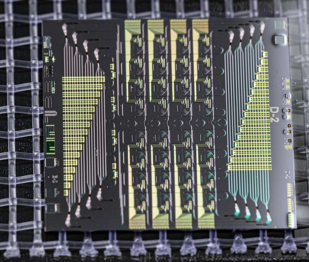
The chip developed by the Oxford team takes advantage of the fact that different polarisations – or waves – of light do not interact with each other. The researchers were able to include several different polarisations on a single chip using nanotechnology, meaning it can process vast amounts of data in parallel without interference.
The potential of photonic chips – which use light rather than traditional electronic circuitry to transfer information – has long been recognised. “We all know that the advantage of photonics over electronics is that light is faster and more functional over large bandwidths,” said June Sang Lee from the department of materials at University of Oxford, first author of a paper in the Science Advances journal which details the work. “So, our aim was to fully harness such advantages of photonics combining with tunable material to realise faster and denser information processing.”
While the authors of the paper admit their work is at an early stage, the number of practical applications for photonic semiconductors on the market is increasing, particularly as businesses look for ways to process large and complex artificial intelligence (AI) workloads.
What is driving the growth in silicon photonic chip adoption?
The most common method of deploying photonics in chip design currently is silicon photonics, which pairs photonic architecture with traditional circuits in a single chip. Gartner says the market for silicon photonics was worth $516m in 2020, and is expected to grow to $2.6bn by 2025.
Three factors are driving this growth says Anushree Verma, director analyst at Gartner. The first, she says, is the “increased interest in artificial intelligence and machine learning workloads, which need faster networking. So we need faster interconnections and higher and higher bandwidth,” which can be provided by integrating photonics.
The other factors relate to chip production, Verma says, with heterogenous integration techniques, which allow photonic and electronic circuits to be married up, being developed by major foundries.
Last year TSMC, the world’s leading chip production company, launched COUPE, a platform for integrating photonics into chips, anticipating booming demand for the technology in data centres. In March, another producer, GlobalFoundries, unveiled GF Fotonix, its own silicon photonics platform, while Intel’s $5.4bn purchase of Tower Semiconductor, announced in February, gives it access to Tower’s silicon photonics foundry in California.
“We’ve seen on the foundry side that heterogeneous integration is now available, which enables integration of chiplets and different designs,” Verma says. “The final driver is the wider availability of electronic photonic design automation tools, which makes it easier for companies to design photonic integrated circuits.” The cost of optical components is also coming down, Verma says, which is aiding adoption.
Photonics could help beat the end of Moore’s Law
Chipmakers need a breakthrough in performance. The looming end of Moore’s Law, the idea that the number of transistors that manufacturers can fit on a single silicon chip doubles every year, means foundries are looking to new technologies. Tech Monitor has reported previously on the potential of new materials such as GaN in semiconductors, and deploying photonics is seen as another potential answer.
Vaysh Kewada is CEO of Salience Labs, a UK start-up developing a silicon photonics chip to power AI workloads. The company, spun out of Oxford and Munster Universities, recently raised $11.5m to fund development of its technology. “There are papers from the 1970s and 1980s of professors thinking about optical processors,” Kewada explains. “But in the last five to seven years silicon photonics as a manufacturing process has come a long way. Now you can go and fabricate a photonic chip in a foundry using standard techniques.”
Companies that get their hands on the technology can benefit from major performance increases. “Photonics is just really fast because light travels fast,” Kewada says. “So you can clock light on a chip at up to 100ghz. Standard processors have been locked on a few gigahertz of clocking speed for the last few years, so that in itself is highly significant.”
Salience claims its approach allows parallel processing to take place in a single chip, meaning data-centre operators could also potentially make energy-efficiency savings. “In electronics, if you want 64 paralysations, you need 64 different chips,” says Kewada. “We can do that on one chip using different wavelengths of light, which means we deliver much higher throughput for a given power envelope.”
The company is far from the only photonic chip producer attracting attention. Silicon photonics start-ups raised $750m in 2020, according to data from Pitchbook, and in April, US company Ayar Labs raised $130m from investors including chipmaker Nvidia.
Beyond the data centre, photonic techniques are being used to power supercomputers and quantum computers. British quantum company ORCA, which recently supplied the UK government with its first quantum computer, is one of a number of businesses globally using photonic technology to create and stabilise qubits, which power quantum machines. The technology is also being deployed as part of Lidar systems used in autonomous vehicles, as well as devices such as sensors.
The future of photonic chips
The price of silicon photonic chips remains high, Gartner’s Verma says, hindering adoption to date. And while manufacturing has become more simple, she argues the ecosystem around the technology is still “nascent”.
“When you add photonic chips into a system, testing results go haywire,” she explains. “So it’s not the same as a normal chip and that process needs to be standardised, which is what the foundries and vendors are trying to do. At the moment processes like this have to be custom-built, and until they are standardised and standard libraries are set up, [photonic chips] will always be costly.”
But widespread interest from beyond the semiconductor industry is likely to ensure the ecosystem develops and prices are driven down, says Jorn Smeets of PhotonDelta, a non-profit organisation based in the Netherlands set up to promote the development of a photonic chip ecosystem in Holland and across Europe.
PhotonDelta recently secured €1.1bn in public and private funding to support photonic chip companies, and works with MIT to produce a roadmap for the development of photonic semiconductors. Smeets says interest in silicon photonics, as well as other photonic production methods such as indium phosphide and silicon nitride, has never been higher.
“We definitely see a trend in interest in this technology,” he says. “It’s not just from the semiconductor manufacturers, but we’re seeing in private equity that banks are starting to get in step and fund companies in this field. Businesses like Meta, Google and Microsoft are all taking part in the roadmap we produce with MIT and the standards work we are doing in the Netherlands, and they’re all very keen because they can potentially reduce energy consumption in their data centres, which is a huge cost for these guys.”
Photonics “is never going to replace electronic circuits,” Smeets adds. “But for these specific applications and markets it can deliver functionalities which can’t be achieved with electronics. We envision a future where you have several components on a single chip, and one of these will be a photonic circuit.”
Read more: Why is there a global chip shortage and when will it end?


