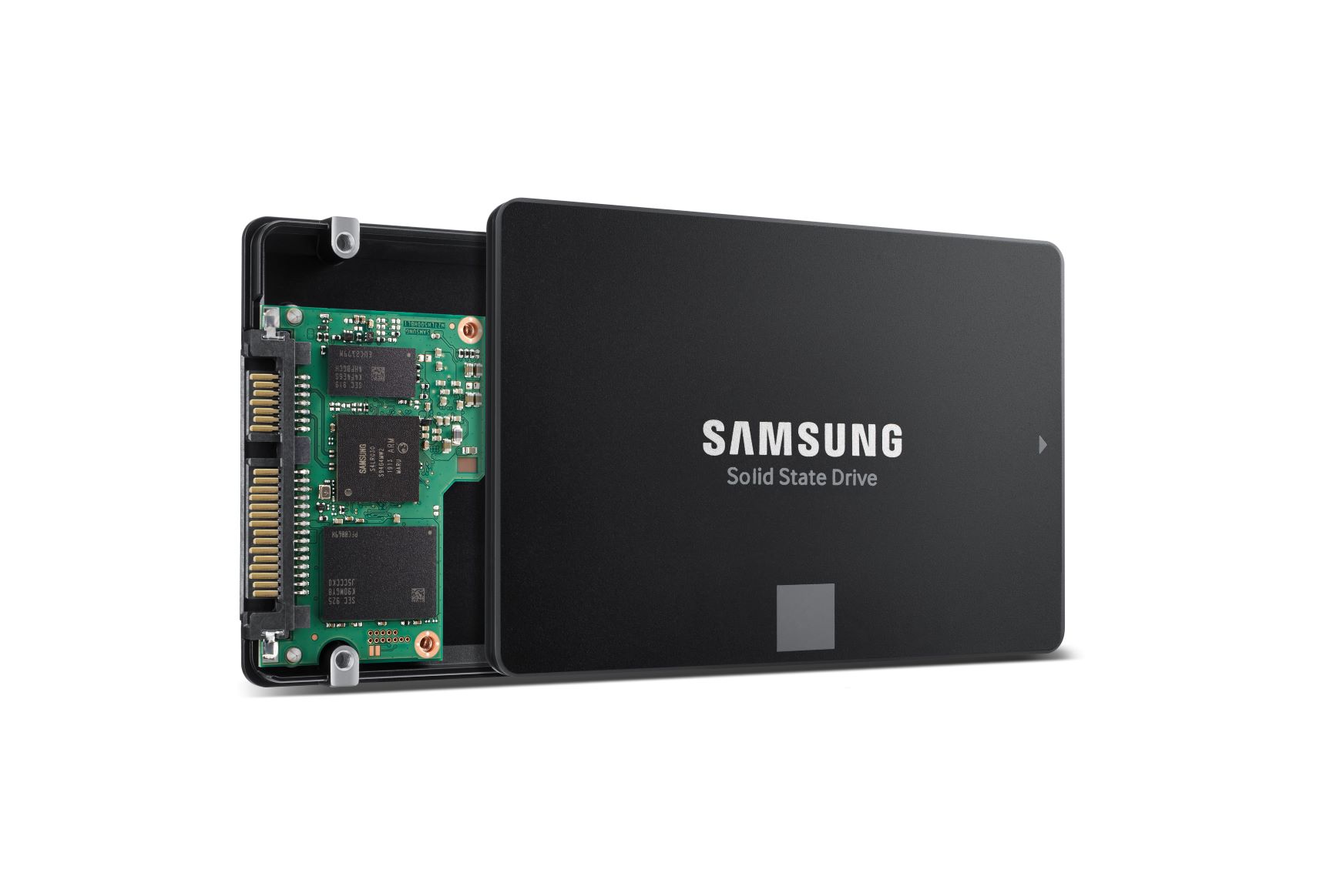
Samsung says it has slashed time to mass production for its latest generation of vertically stacked solid state drives (V-NAND SSDs) by four months, as its fabrication labs started work on the company’s new 250GB SATA SSDs this week.
These boast 100-layers of NAND cells for the first time, and a writing speed of 450 microseconds, with a reading response time of 45 microseconds.
Performance is up 10 percent, the company said, and power consumption down 15 Percent compared to 90-layer V-NANDs. The SSDs will ship to global PC OEMs.
The start of mass production comes as NAND oversupply has led to a pricing war among suppliers; prices are expected to rebound in early 2020.
New Samsung SSD: From Conception to Mass Production in 13 Months
The launch of mass production this week means that the company launched its latest generation of V-NAND in just 13 months, Samsung said; an important win for the company in an aggressively competitive market.
“By bringing cutting-edge 3D memory technology to volume production, we are able to introduce timely memory lineups that significantly raise the bar for speed and power efficiency,” said Kye Hyun Kyung, executive VP of product and development.
He added: “With faster development cycles, we plan to rapidly expand the markets for our high-speed, high-capacity 512GB V-NAND-based solutions.”
New Manufacturing Techniques
Manufacturing uses Samsung’s “channel hole etching” technology, allowing it to add around 40-percent more cells to the previous nine-layer single-stack structure. The company does this by building an electrically conductive mould stack of 136 layers, then vertically piercing cylindrical holes from top to bottom, creating uniform 3D charge trap flash (CTF) cells, it said in a release pushed out late Monday.
(CTF allows a cell-to-cell interference-free structure. It is based on a non-conductive layer of silicon nitride that temporarily traps electrical charges to maintain cell integrity. This layer has been modified into a three-dimensional form that wraps around the control gate of the cell, acting as an insulator that holds charges, thereby preventing data corruption caused by cell-to-cell interference.)
As the mould stack in each cell area increases in height, NAND flash chips tend to become more vulnerable to errors and read latencies.
To tackle this issue, the company has incorporated a circuit design that allows it to achieve the industry’s fastest data transfer speed; a design that also means it will be able to offer V-NAND SSDs with over 300 layers simply by mounting three of the current stacks, without, it claims, compromising chip performance or reliability.
Samsung plans to offer 512GB three-bit V-NAND SSD and eUFS flash storage in the second half of this year. It says it will ramp up production of higher-speed and greater-capacity sixth-generation V-NAND solutions at its Pyeongtaek campus starting next year to better meet demand from global customers.


