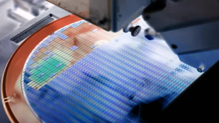
Intel has confirmed that two high numerical aperture (NA) lithography machines from ASML are now in operation at its manufacturing facilities, with initial production data suggesting improved reliability compared to earlier models. The semiconductor company, which became the first in the industry to receive ASML’s high NA machines last year, reported that these systems have already processed 30,000 wafers in a single quarter. Wafers, the foundational material for semiconductor production, are used to fabricate computing chips at scale.
Intel senior principal engineer Steve Carson, speaking at a conference in San Jose, California, outlined the performance of the new systems, stating that the high NA lithography machines have demonstrated approximately twice the reliability of previous extreme ultraviolet (EUV) models. “We’re getting wafers out at a consistent rate, and that’s a huge boon to the platform,” Carson said.
The deployment of ASML’s advanced lithography technology represents a strategic shift for Intel, which had faced setbacks in previous technology transitions. The company had been slower than competitors, including Taiwan Semiconductor Manufacturing Company (TSMC), in adopting the prior generation of EUV lithography tools. The integration of those systems had taken Intel seven years, contributing to delays in its manufacturing roadmap.
ASML’s high NA lithography machines are claimed to introduce efficiencies in semiconductor production by reducing the number of exposures required during the photolithography process. Carson explained that operations that previously involved three exposures and approximately 40 processing steps can now be completed with a single exposure and a reduced number of steps. The streamlined process is expected to enhance production throughput and lower complexity.
Intel prepares for 18A and 14A manufacturing using high NA EUV
Intel plans to test the high NA lithography systems in its 18A manufacturing process, which is slated for mass production later this year alongside a new generation of PC chips. The company has also indicated that the machines will be integrated into its future 14A manufacturing technology, though a timeline for full-scale deployment has not yet been disclosed.
ASML’s EXE platform, the latest generation of its high NA EUV lithography technology, is designed to enhance resolution and transistor density for advanced semiconductor manufacturing. According to ASML, EXE systems improve resolution by increasing the NA from 0.33 in NXE systems to 0.55. This advancement enables an 8 nm critical dimension, allowing for transistors that are 1.7 times smaller and 2.9 times denser than those produced using NXE systems.
The higher NA required larger mirrors, which altered the angle at which light strikes the reticle, reducing reflectivity and making pattern transfer more challenging. Instead of switching to larger reticles, ASML adopted an anamorphic optics approach, demagnifying patterns by 4x in one direction and 8x in the other. This design preserves traditional reticle sizes while improving resolution, allowing chipmakers to adopt the technology without significant changes to existing manufacturing processes.
Last month, ASML reported stronger-than-expected financial results for the fourth quarter of 2024, driven by continued demand for its advanced semiconductor manufacturing equipment. The company posted net sales of €9.3bn, surpassing its prior guidance, with a gross margin of 51.7% and net income of €2.7bn. Order activity also saw a significant increase, with net bookings reaching €7.1bn, more than doubling from the €2.6bn recorded in the third quarter. Of these orders, €3bn were attributed to EUV systems, highlighting ongoing investment in high-precision lithography technology.


