Nvidia processors are among the most widely used in artificial intelligence training and now the chip design giant has shown AI could be invaluable in improving the design of those and other semiconductors. In a new research paper, Nvidia found a combination of AI techniques could lead to better transistor placement and builds on a 2021 paper by Google.

The placement of transistors on a chip has a major impact on its cost, speed and power consumption. There are tens of billions on a single piece of silicon and any efficiency improvement can lead to significant gains for the company.
Companies use design software that optimises the placement of the transistors to ensure peak performance and the new research by Nvidia says AI can be used to better predict the exact place each transistor should be, including ways to place large groups of transistors.
Bill Dally, Nvidia chief scientist, said chip manufacturing improvements using conventional software techniques are slowing with per-transistor costs in new generations of chip technology higher than previous generations, breaking “Moore’s Law”, established by the late Intel co-founder Gordon Moore, that states chips will always get cheaper and faster.
Dally told Reuters “You’re no longer actually getting an economy from that scaling,” adding that to continue moving forward and delivering value for customers “we have to get it by being more clever on the design” as cheaper transistors are no longer a viable approach.
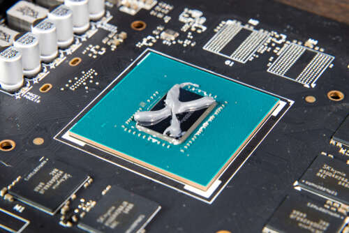
Nvidia’s open-source solution for AI chip design
In the paper, AutoDMP: Automated DREAMPlace-based Macro Placement, the Nvidia scientists were able to demonstrate that AI could be used to optimise a chip design with 2.7 million cells and 320 macros in under three hours on a single Nvidia DGX Station A100 processor. The researchers wrote that this “demonstrates the promise and potential of combining GPU-accelerated algorithms and ML techniques for VLSI [integrated circuit] design automation”.
The researchers used reinforcement learning with a second layer of AI to improve the process of placing the transistors, as well as blocks of transistors. It analysed the sizes of different transistors to search through the design space and select where each individual and group should go to make the most out of every section of the silicon.
The results achieved through the AI design software were comparable to commercial tools and superior to open-source academic tools for chip design. It is also more efficient in terms of computation power which could be the key to improving the manufacturing process as the price of placement increases.
The AutoDMP method is being open-sourced by Nvidia to “improve the quality of mixed-size placement”. Using the AI tool the placement space is automatically and efficiently explored by the AI using a GPU-accelerated placement engine that generates placement solutions in just a few hours.
The researchers say it can help improve the turnaround time for early-stage architectural exploration. This allows chip designers to more rapidly iterate through options while coming up with the most efficient solution and accurately outline “floorplan modification decisions” on each chip.
Read more: New Nvidia DGX quantum computing system unveiled at GTC 2023