Semiconducter firm Altatech has introduced its new AltaSight LEDMax system for detecting, classifying and characterising defects on wafers used in manufacturing LEDs.
AltaSight LEDMax improves production yields for LED devices by accurately detecting process-induced defects, including those that can result during metal-organic chemical vapour deposition (MOCVD) of epitaxial layers, subsequent patterning processes and final inspection.
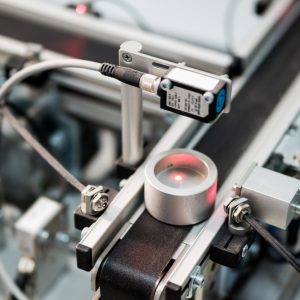
The non-contact system generates images of surface imperfections with resolution down to 1 micron and a unique depth-of-focus capability approaching 500 microns, using Altatech’s patented sensor technology that filters out all background noise.
AltaSight LEDMax combines up to three inspection modules, allowing it to be used in volume manufacturing, process development or R&D applications, handles the full range of compound semiconductor wafers and the new LEDMax has the versatility to meet other III-V inspection requirements.
In addition, the LEDMax can accommodate sapphire, silicon, silicon carbide and other transparent surface substrates and can handle four- to eight-inch wafers without any hardware changes, and a field-upgradeable option for handling two-inch substrates.
Altatech Semiconductor president Jean-Luc Delcarri said with its multi-class defect reporting and high accuracy, our newest inspection system meets the unique needs of LED manufacturers.
"Altatech is entering this market by providing a defect-detection solution that traditional semiconductor-inspection tools cannot match in terms of reliability and cost-efficiency," said Delcarri.