Diversified technology company 3M and IBM plan to jointly develop a new type of electronic glue to build stacks of semiconductors – 3D chips.
Stacking of semiconductors is expected to allow high level of integration of information technology and consumer electronics applications.
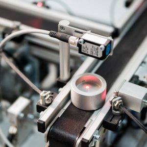
IBM will create semiconductor packaging processes and 3M will develop and manufacture adhesive materials, under the agreement.
IBM Research VP Bernard Meyerson said today’s chips, including those containing ‘3D’ transistors, are in fact 2D chips that are still very flat structures.
"Our scientists are aiming to develop materials that will allow us to package tremendous amounts of computing power into a new form factor – a silicon ‘skyscraper,’ Meyerson said.
"We believe we can advance packaging, and create a new class of semiconductors that offer more speed and capabilities while they keep power usage low – key requirements for many manufacturers, especially for makers of tablets and smartphones."
3M Electronics Markets Materials Division vice president Herve Gindre said the company looks forward to working alongside IBM.
"3M has worked with IBM for many years and this brings our relationship to a new level. We are very excited to be an integral part of the movement to build such revolutionary 3D packaging," Gindre said.